UC Berkeley Press Release
Goal of nanoscale optical imaging gets boost with new hyperlens
BERKELEY – Scientists at the University of California, Berkeley, have developed a "hyperlens" that brings them one major step closer to the goal of nanoscale optical imaging.
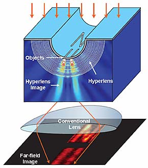
 Schematic of an optical hyperlens that can magnify and project sub-diffraction-limited objects onto a far-field plane. The objects and the hyperlens are enlarged to show details; they are actually much smaller than a conventional lens. (Images courtesy the Zhang Lab, UC Berkeley) |
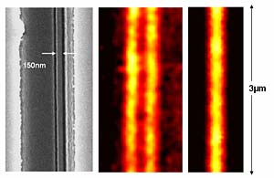
The new hyperlens, described in the Feb. 23 issue of the journal Science, is capable of projecting a magnified image of a pair of nanowires spaced 150 nanometers apart onto a plane up to a meter away.
Currently, to capture details down to a few nanometers, scientists must use scanning electron or atomic force microscopes, which create images by scanning objects point by point. Scanning electron microscopes can take up to several minutes to get an image. Because the object must remain immobile and in a vacuum during this process, imaging is restricted to non-living samples.
Optical microscopes, in contrast, can snap an entire frame of an image in a single shot. They are commonly used in biological laboratories to study living cells, as well as in the high-tech industry to create integrated circuits, or in telecommunications. But the ability to resolve nanometer-level detail in optical imaging has been constrained by the so called "diffraction limit," a fundamental limit in optics related to the type of light waves emitted from an object.
Propagating waves can travel far and be collected by an optical lens, including the human eye, to form an image. Evanescent waves contain far greater detail and resolution of an object, but they decay too quickly for conventional lenses to capture them.
"Capturing the information carried by the evanescent waves is the Holy Grail of optical imaging," said Xiang Zhang, UC Berkeley professor of mechanical engineering and principal investigator of the study. "The hyperlens shows a new way to beat the diffraction limit, which would allow biologists to not only see a cell's nucleus and other smaller components, but to study the movement and behavior of individual molecules in living cells in real time. In technology, this could eventually lead to higher density integrated circuits and DVDs."
 Hyperlens imaging of a pair of nanowires 35 nm wide and spaced 150 nm apart. On the left is a scanning electron microscope image of the lines. In the middle is the magnified hyperlens image showing the 150 nm spaced line pair. Without the hyperlens, the two lines cannot be distinguished, as in the image taken in a control experiment shown to the right. |
"In this experiment, the loss of the evanescent waves results in a diffraction limit of 260 nanometers," said Zhaowei Liu, UC Berkeley postdoctoral researcher in mechanical engineering and co-lead author of the paper. "The hyperlens breaks this limit by capturing an image of objects smaller than 150 nanometers."
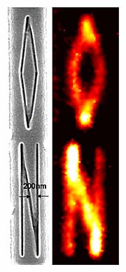
The researchers used nanowires that were 35 nanometers wide and inscribed onto an inner layer of chrome that sits atop the hyperlens. In the first experiment, two nanowires were placed parallel to each other 150 nanometers apart. The researchers also shaped nanowires into the letters O and N for another demonstration.
The hyperlens consists of multiple layers of silver and aluminum oxide placed along the cavity of half a cylinder carved out of quartz. When an object is illuminated, its evanescent waves travel through the lens. As the wave vectors move outward, they are progressively compressed. This compression allows the image of the objects to be magnified by the time it reaches the outer layers of the hyperlens. At this point, it can be captured by a conventional optical lens and projected outward onto a far-field plane a meter away.
Zhang's group began the quest to beat the diffraction limit six years ago. In 2005, Zhang led a research team that developed a superlens capable of capturing evanescent waves and imaging an object at a half-pitch resolution of 60 nanometers.
The researchers point out that, unlike the hyperlens, the superlens does not alter the nature of the evanescent waves, so once the waves leave the lens, they decay quickly. This exponential loss of the evanescent waves required the image plane to sit close to the lens.
 Shown on the left is a scanning electron microscope image of nanowires shaped in the letters O and N. To the right is the hyperlens image of the nanowires. |
"The superlens we showed before is near-sighted - the projected image only exists near the surface of the lens with no magnification," explained Liu. "That limits the practical applications for the superlens, since the camera needs to be within an object's 'near-field' range. To make a lens useful for far-field imaging below a diffraction limit, you must convert evanescent waves to propagation waves, which is what the hyperlens does."
Zhang noted that while the hyperlens can project a magnified image of a sub-diffraction object up to a meter away, the object that is being imaged still needs to be placed in the near-field zone of the lens. "We have not yet reached the goal of making a far-field optical nanoscope," he said. "But we are one major step closer."
Recently, Zhang's group demonstrated another type of far-field superlens by using surface grating to convert evanescent waves into propagating waves.
"It is too early to say which approach - the hyperlens or the far-field superlens - will be used first for practical applications," said Zhang. "We are continuing to work on a number of approaches to create far-field images below the diffraction limit."
Hyesog Lee, a graduate student in mechanical engineering, is the co-lead author of the paper. Other co-authors are graduate student Yi Xiong and research scientist Cheng Sun, all in Zhang's laboratory. Zhang is also a faculty scientist at Lawrence Berkeley National Laboratory and the Center for Information Technology Research in the Interest of Society (CITRIS) at UC Berkeley.
The Army Research Office, the Air Force Office of Scientific Research and the National Science Foundation supported this research.

