|
HOME | SEARCH | ARCHIVE |
|
Campus introduces journalists to world of nanotechnology
![]()
By Diane Ainsworth, Public Affairs
| | 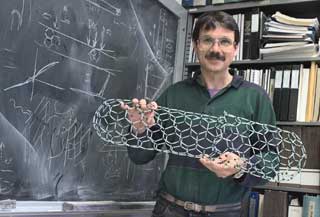 Physics Professor Alex Zettl displays a model of a carbon nanotube, a strong form of carbon that scientists believe may help them build miniaturized electronic circuits. Lawrence Berkeley Lab photo |
07 March 2001
|
One day those strange, hair-like carbon threads under Alex Zettl’s scanning tunneling microscope may play the same role that silicon does today in electronic circuits: they could become the circuitry for networks of microsensors, miniature electronic circuits, sugar-cube-sized computers and motion or light detectors no bigger than a speck of dust. The technology isn’t that far off, but Zettl, the Berkeley physics professor who helped design the state-of-the-art microscope for Lawrence Berkeley National Laboratory, knows his work to build these ultra-fine connectors is about to uncork the bottled genie. Zettl, who is helping to lead the next revolution in semiconductor miniaturization, presented his nanotechnology work to this year’s National Association of Science Writers conference, which convened last month at the Clark Kerr Campus. About 100 print and broadcast journalists from around the world, visiting San Francisco for the annual American Association for the Advancement of Science meetings across the bay, joined the conference. The opening session, titled “Small Is Beautiful,” introduced participants to Berkeley’s research expertise in the field. “Berkeley is a leader in this emerging field, with some 90 scientists involved in some way in nanotechnology research, in disciplines such as engineering, physics, chemistry and molecular and cell biology,” said Robert Sanders, senior science writer in Berkeley’s Office of Public Affairs, who helped coordinate the campus workshop. “We wanted to showcase that expertise for science writers and journalists who want to stay on top of the field. And it worked out very well; the workshop was sold out.” Nanotechnology is all about molecular manufacturing or, more simply, building things one atom or molecule at a time. A nanometer is one-billionth of a meter, or just three to four atoms wide. Based on a scientist’s understanding of the chemical properties of atoms and molecules — how they “stick” together — nanotechnology research focuses on the construction of novel molecular devices that possess extraordinary properties. The trick to advancing the field, researchers say, is to be able to move atoms individually and build structures that can be turned into miniature robots and machines. The explosion has just begun. Researchers and private companies are scrambling to invent devices that can be manufactured at almost no cost by treating atoms discretely, like computers treat bits of information, according to the experts. This would allow the manufacturing industry to build consumer products automatically, without traditional labor, just like a Xerox machine now produces unlimited copies of written documents without the aid of a human being to retype the original information. The ability to do that is almost within the grasp of scientists, some believe. In the next 10 to 15 years, physicists like Zettl will be using their scanning tunneling microscopes and mass spectrometers to help them manipulate atoms and learn more about their behavior on surface materials. The electrical properties of these new nanoscale materials will make them conduits for increasingly small devices, Roco said. Speaking at the science writers conference, Roco and Berkeley chemist Paul Alivisatos, electrical engineer Kris Pister and bioengineer and materials scientist Kevin Healy discussed such science fantasies as “smart” buildings that would be wired with accelerometers to make them earthquake-resistant; giga- and- terabit information processors that would allow the manufacture of tiny televisions and computers; and automobiles with sensors to anticipate collisions and deploy airbags before they occur. Visions of medicine 25 years from now might even include the manufacture of synthetic materials that are capable of instructing cells to regenerate and repair damaged tissues and organs, such as the heart, liver, bone and cartilage, Healy said.
“Nanotechnology is leading researchers to ways of building computers, microcircuits and machines on fine scales no larger than the length of a few atoms,” said workshop presenter Mihail Roco, a senior adviser for nanotechnology at the National Science Foundation and a key architect of the National Nanotechnology Initiative. “This field is going to be central to science and engineering and allow us to build the smallest structures imaginable.”
Home | Search | Archive | About | Contact | More News
Copyright 2000, The Regents of the University of California.
Produced and maintained by the Office of Public Affairs at UC Berkeley.
Comments? E-mail berkeleyan@pa.urel.berkeley.edu.